Background
About FPGAs
Field Programmable Gate Arrays (FPGAs) are integrated circuits containing arrays of gates which are programmable in the field. Most chips you will encounter, have transistor gates arranged in a fixed order, thus providing a fixed functionality. Conversely, FPGAs can change their internal connections by simply loading new configurations. Fundamentally, configurations program lookup tables (LUTs), which form the basic building blocks of logic. These lookup tables are so important to the design and usage of an FPGA that they usually form part of the name of the part. For example, Fomu uses a UP5K, which has about 5000 LUTs. NeTV used an LX9, which had about 9000 LUTs, and NeTV2 uses a XC7A35T that has about 35000 LUTs.
FPGA LUTs are almost always n-inputs to 1-output. The ICE family of FPGAs from Lattice have 4-input LUTs. Xilinx parts tend to have 5-input or 6-input LUTs which generally means they can do more logic in fewer LUTs. Comparing LUT count between FPGAs is a bit like comparing clock speed between different CPUs; not entirely accurate, but certainly a helpful rule of thumb.
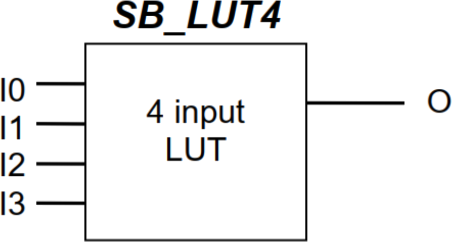
The ICE40 LUT4 is a basic 4-input 1-output function table.
The basic building block of Fomu is the SB_LUT4. It
has four 1-bit inputs and one 1-bit output. To program Fomu, we must define what
each possible input 4-bit pattern will create on the output. To do this, we turn to
a truth table:
0 |
1 |
2 |
3 |
4 |
5 |
6 |
7 |
8 |
9 |
10 |
11 |
12 |
13 |
14 |
15 |
|
|---|---|---|---|---|---|---|---|---|---|---|---|---|---|---|---|---|
IO0 |
0 |
0 |
0 |
0 |
0 |
0 |
0 |
0 |
1 |
1 |
1 |
1 |
1 |
1 |
1 |
1 |
IO1 |
0 |
0 |
0 |
0 |
1 |
1 |
1 |
1 |
0 |
0 |
0 |
0 |
1 |
1 |
1 |
1 |
IO2 |
0 |
0 |
1 |
1 |
0 |
0 |
1 |
1 |
0 |
0 |
1 |
1 |
0 |
0 |
1 |
1 |
IO3 |
0 |
1 |
0 |
1 |
0 |
1 |
0 |
1 |
0 |
1 |
0 |
1 |
0 |
1 |
0 |
1 |
O |
? |
? |
? |
? |
? |
? |
? |
? |
? |
? |
? |
? |
? |
? |
? |
? |
For example, to create a LUT that acted as an AND gate, we would define
O to be 0 for everything except the last column. Conversely, to create
a NAND gate, we would define O to be 1 for everything except the last column.
It is from this simple primitive that we create the building logic blocks of
FPGA design.
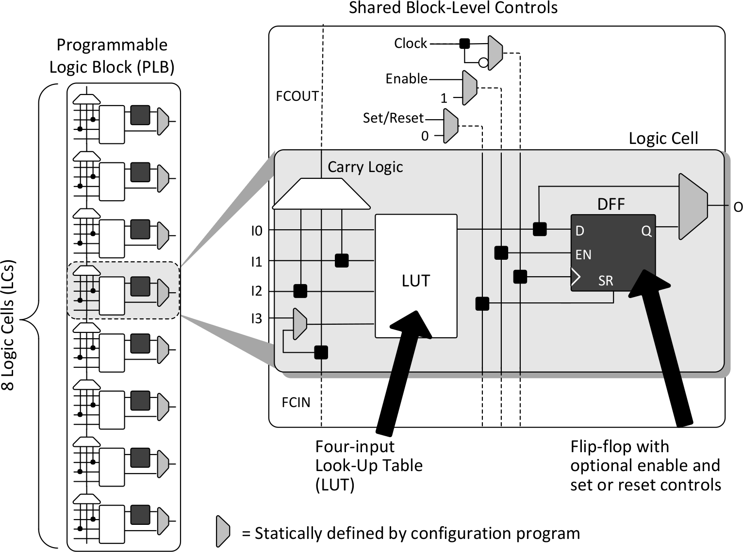
Programmable Logic Block (PLB), Block Diagram.
Modern FPGA devices are no longer composed of arrays of gates (i.e. LUTs) only. Typically, LUTs are grouped with flip-flop registers (DFF) and some carry logic, in so-called Programmable Logic Blocks (PLBs) or Configurable Logic Blocks (CLBs); depending on the vendor. These resources allow combining multiple LUTs for describing larger logical functions and for providing sequential behaviour.
Furthermore, additional purpose-specific blocks are included in the devices: Block RAMs (BRAMs), Digital Signal Processing (DSP) blocks, high-performance serial transmitters/receivers, etc. Those so-called hard blocks allow better area and power usage than LUT-based components. Nevertheless, the behaviour of any of those hard blocks can be replicated using PLBs only. At the same time, custom behaviour can only be described through LUTs, because all hard blocks are programmable within the pre-fixed functionality only.
Turning code into gates
Configuring all the LUTs, carry logic and other hard blocks manually is hard and very challenging; so people have come up with abstract Hardware Description Languages (HDLs), that allow us to describe the expected behaviour and/or structure. The two most common languages are Verilog and VHDL. However, a modern trend is to achieve hardware description by embedding a Domain Specific Language (DSL) inside an existing programming language, such as how Migen is embedded in Python, Clash is embedded in Haskell, or Chisel and SpinalHDL are embedded in Scala.
Here is an example of a counter module with a registered output:
module example (
  input C,
  output reg [0:5] Q
);
  reg [0:8] counter;

  always @(posedge C)
  begin
    counter <= counter + 1'b1;
  end

  always @(posedge C)
  begin
    Q <= counter[3] ^ counter[5] | counter<<2;
  end
endmodule
We can run this HDL module through a synthesizer to turn it into LUT and DFF blocks, or we can turn it into a more familiar logic diagram:
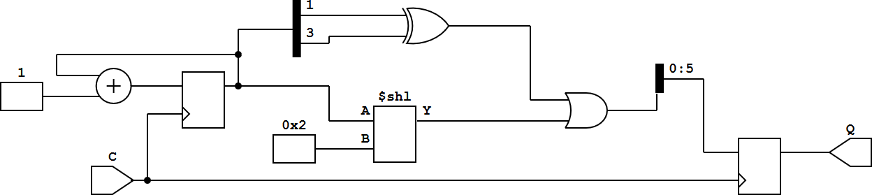
A synthesis of the above logic into basic blocks.
Turning gates into a bitstream
If we do decide to synthesize to PLBs, we will end up with a pile of LUTs and DFFs that need to be strung together somehow. This is done by a Place-and-Route (PnR) tool. This performs the job of assigning physical PLBs to each LUT and DFF that gets defined by the synthesizer; and then figuring out how to wire it all up.
Once the PnR tool is done, it generates an abstract file that needs to be translated into a format that the hardware can recognize. This is done by a bitstream packing tool.
Loading a bitstream into a device
Finally, the bitstream needs to be loaded onto the device somehow. It can be done manually by toggling wires of the FPGAs programming interface. However, most FPGAs are volatile, which means the configuration is lost when unplugged. Therefore, most FPGA boards include some flash memory, which is typically programmed through SPI. Then, when the FPGA is plugged again, it loads the configuration from a predefined location in the flash.
About the ICE40UP5K
We will use an ICE40UP5K for this workshop. This chip has a number of very nice features:
5280 4-input LUTs (LC)
16 kilobytes BRAM
128 kilobytes “SPRAM”
1x Current-limited 3-channel LED driver
2x I2C and 2x SPI interfaces
8x 16-bit DSP units
Warmboot capability
Open toolchain
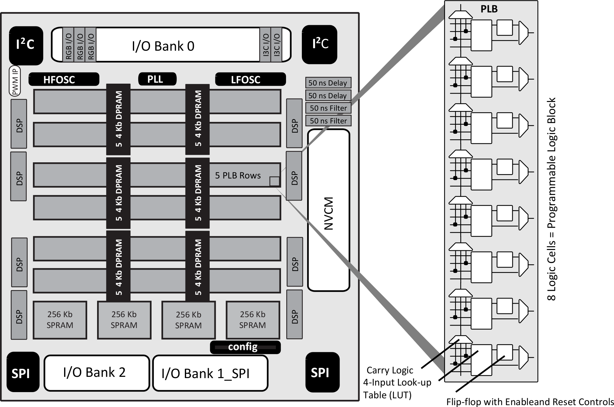
iCE40UP5K Device, Top View.
BRAM is frequently used to store data such as buffers, CPU register files, and large arrays of data. This type of memory is frequently reused as RAM on many FPGAs. The ICE40UP5K is unusual in that it also has 128 kilobytes of Single Ported RAM that can be used as memory for a softcore (a term used for a CPU core running inside an FPGA, to differentiate it from a ‘hard’ - i.e. fixed chip - implementation). That means that, unlike other FPGAs, valuable block RAM isn’t taken up by system memory.
Additionally, the ICE40 family of devices generally supports warmboot capability. This enables us to have multiple designs live on the same FPGA and tell the FPGA to swap between them.
As always, this workshop wouldn’t be nearly as easy without the open source tools that enable us to port it to a lot of different platforms.
About Fomu
Fomu is an ICE40UP5K that fits in your USB port. It contains two megabytes of SPI flash memory, four edge buttons, and a three-color LED.
Unlike most other ICE40 projects, Fomu implements its USB in a softcore. That means that the bitstream that runs on the FPGA must also provide the ability to communicate over USB. This uses up a lot of storage on this small FPGA, but it also enables us to have such a tiny form factor, and lets us do some really cool things with it.
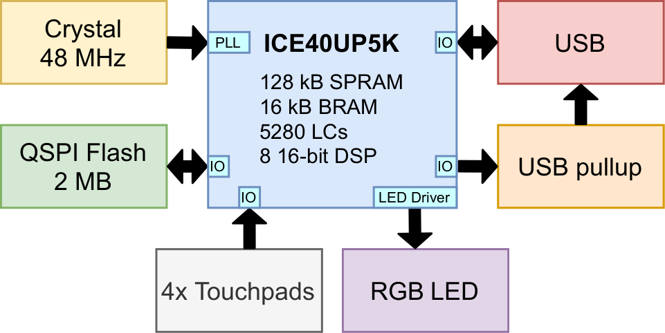
Block diagram of Fomu.
The ICE40UP5K at the heart of Fomu really controls everything, and this workshop is all about trying to unlock the power of this chip.
Note
Some figures in this section were extracted from the iCE40 UltraPlus Family Data Sheet.